Hardware Circuit Design and Signal Integrity
Assurance
The core challenge of HART hardware design lies in how to simultaneously carry a 4-20 mA DC analog signal, a 1200/2200 Hz FSK AC signal, and possible loop supply voltage on the same pair of wires, ensuring that the three do not interfere with each other and meet stringent industrial EMC standards. This chapter starts with the system architecture and analyzes the design key points layer by layer.
1.1 System Architecture and Signal Link
A typical HART slave device (such as a smart transmitter) follows this signal topology:
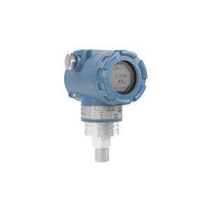
MCU → HART chip → Coupling circuit → 4-20 mA DAC → Current loop (250 Ω load).

The MCU communicates with the HART chip via a UART interface, sending the digital data to be modulated. The HART chip converts the UART data stream into an FSK signal output. The coupling network (usually a capacitor-resistor network or transformer coupling) injects the FSK AC signal into the 4-20 mA current loop while blocking the DC component. The DAC converts the sensor data into a precise 4-20 mA analog current output. The receiving link proceeds in the opposite direction: the FSK signal is coupled from the loop to the HART chip for demodulation, restoring the UART data stream back to the MCU.
1.2 Coupling Circuit and Signal Superposition Design
The coupling circuit is a critical node for HART signal integrity. Its design goals include: providing a low-impedance path for FSK signals (1200-2200 Hz); providing high isolation for DC and low-frequency analog signals; and suppressing high-frequency noise and harmonic interference.
The recommended coupling solution is an RC high-pass filter network. Typical parameters are: coupling capacitor 0.047μF - 0.1μF (voltage withstand ≥50 V), and series resistor value adjusted according to signal amplitude requirements. The -3dB cutoff frequency of the coupling network should be designed below 800 Hz to ensure minimal attenuation of the 1200 Hz fundamental frequency signal; refer to the manufacturer's datasheet for details. For high-precision applications, a transformer coupling scheme can be used, which offers complete electrical isolation and common-mode noise suppression, but is relatively more expensive and larger.
1.3 Key PCB Layout Specifications
PCB layout directly impacts the signal integrity and EMC performance of a HART system. The following are key design specifications validated in mass production:

Zoned Layout:Strictly enforce physical isolation between the digital zone (MCU, clock circuit), analog zone (HART chip, DAC, coupling circuit), and power zone. Establish complete ground plane isolation bands between each zone.
Grounding Strategy:Employ either star grounding or a solid ground plane solution. Digital and analog grounds should converge at a single point at the power input to avoid ground loop coupling.
Impedance Control: Impedance Control: The characteristic impedance of HART signal traces is controlled within 50 Ω ± 10%. Trace lengths are kept as short as possible, avoiding right-angle bends to reduce signal reflection and crosstalk.
Decoupling Design: A 0.1 μF ceramic decoupling capacitor is placed near the power supply pin of each active device. A 10 μF tantalum capacitor is added to the power supply pins of the DAC and HART chips to ensure power supply ripple <10 mVpp.
Shielding Measures: Grounding protection lines (Guard Rings) are placed on both sides of sensitive analog traces. Grounding copper foil is laid in critical areas, and metal shielding covers are used when necessary.
2 Protocol Stack Development and System Integration Path
The development of the HART protocol stack is the most technically complex part of the entire project cycle. Developing a complete protocol stack independently requires a deep understanding of the HART specification documents (HCF_SPEC-99, HCF_SPEC-127, etc.), and the development cycle typically ranges from 6 to 12 months, facing the dual challenges of compatibility testing and on-site interoperability verification. For most application scenarios, adopting a mature commercial protocol stack is a more pragmatic choice.
2.1 Comparison of Commercial Protocol Stack Solutions
Table 1.Comprehensive Comparison of Commercial HART Protocol Stack Solutions
| Protocol Stack Solution | Supplier | Certification Status | Core Advantages | Potential Limitations |
| HART official stack | FieldComm Group | Official certification | Highest authority, synchronized protocol specification updates, best global compatibility | Higher licensing fees, incomplete source code |
| ADI HART Stack | Analog Devices | ADI internal certification | Deeply optimized with ADI chips, mature performance tuning, comprehensive documentation | Integrated with the ADI hardware ecosystem, technical support, longer response time. |
| Microcyber HART Stack | Microcyber | Official certified | English technical documentation, short integration cycle. | Supports customized development of specific advanced functions. |
Selection recommendations: For commercial projects requiring rapid time-to-market, we recommend prioritizing Microcyber's HART Stack—it boasts comprehensive technical documentation, a strong technical support team, and deep optimizations for domestically produced chips, reducing the protocol stack integration cycle to 2-4 weeks. For projects with an existing ADI hardware ecosystem, the ADI HART Stack offers the most mature chip-level collaborative optimization, but its technical support response time is relatively longer.
2.2 Development Process and Debugging Strategy
For HART project development based on a commercial protocol stack, the following standardized process is recommended:

[1] Low-level driver development: Complete the UART driver (1200 bps baud rate, 1 start bit + 8 data bits + 1 parity bit + 1 stop bit), HART chip initialization configuration, and DAC register mapping.
[2] Protocol stack integration: Port the commercial protocol stack to the target MCU platform, configure the device description (DD) file, and implement the general command set (command 0-command 48) response.
[3] Command implementation: Implement the application layer command processing logic line by line, including process variable reading and writing, device configuration parameter management, and self-diagnostic function reporting.
[4] Joint debugging and testing: Use a HART handheld communicator (such as 475/375) or host computer software to perform point-to-point communication verification and confirm the correctness of command responses.
[5] Conformance testing: Perform compliance verification using FieldComm Group's official conformance testing tools (such as the HART Test System) and obtain a certification certificate.
[6] Field verification: Conduct long-term stability tests in actual industrial environments to verify communication reliability under scenarios such as multi-device networking, long-distance transmission, and electromagnetic interference.
During the debugging phase, it is recommended to equip the system with a HART protocol analyzer, which can capture and parse HART frame data on the bus in real time to quickly locate physical layer signal anomalies or protocol layer response errors.
3、Core Value Created for Customers
The value of HART solutions lies not only in their technological advancements but also in the quantifiable business benefits they bring to end customers. Based on deployment experience of over 40 million HART devices globally, the commercial value of HART technology has been fully validated across multiple dimensions.
Table 7. Core Value Matrix Created by HART Solutions for Customers
Value Dimensions | Specific Benefits | Quantifiable Indicators |
Reduced Deployment Costs | No rewiring required, compatible with 4-20 mA infrastructure | 60%-80% reduction in upgrade costs |
Improved Operational Efficiency | Remote device configuration, online diagnostics, predictive maintenance | 50%+ reduction in on-site inspection frequency |
Ensuring Data Integrity | Digital transmission eliminates analog signal drift and conversion errors | Data accuracy improved to ±0.01% FS |
Extended Asset Lifespan | Real-time monitoring of device health status and fault early warning | 40%+ reduction in unplanned downtime |
Accelerated Time-to-Market | Standardized protocol stack + mature chip solutions shorten R&D cycle | Development cycle shortened by 4-6 months |
Enhanced System Scalability | Supports multi-variable transmission and device cascading networking | Single-point access can be expanded to 15+ device nodes. |
Of particular note is the unique advantage of HART solutions in upgrading existing equipment: traditional 4-20 mA meters can be seamlessly integrated into DCS/PLC systems and industrial internet platforms simply by adding a HART multiplexer in the control room or installing a WirelessHART adapter in the field, achieving "zero-disruption" digital transformation. This feature makes HART an ideal choice for process industry enterprises to achieve gradual digital transformation.